


"Frontiers of Technology · Empowering with Ceramics" — Advanced Semiconductor Processing and Packaging Ceramic Technology Symposium Successfully Held
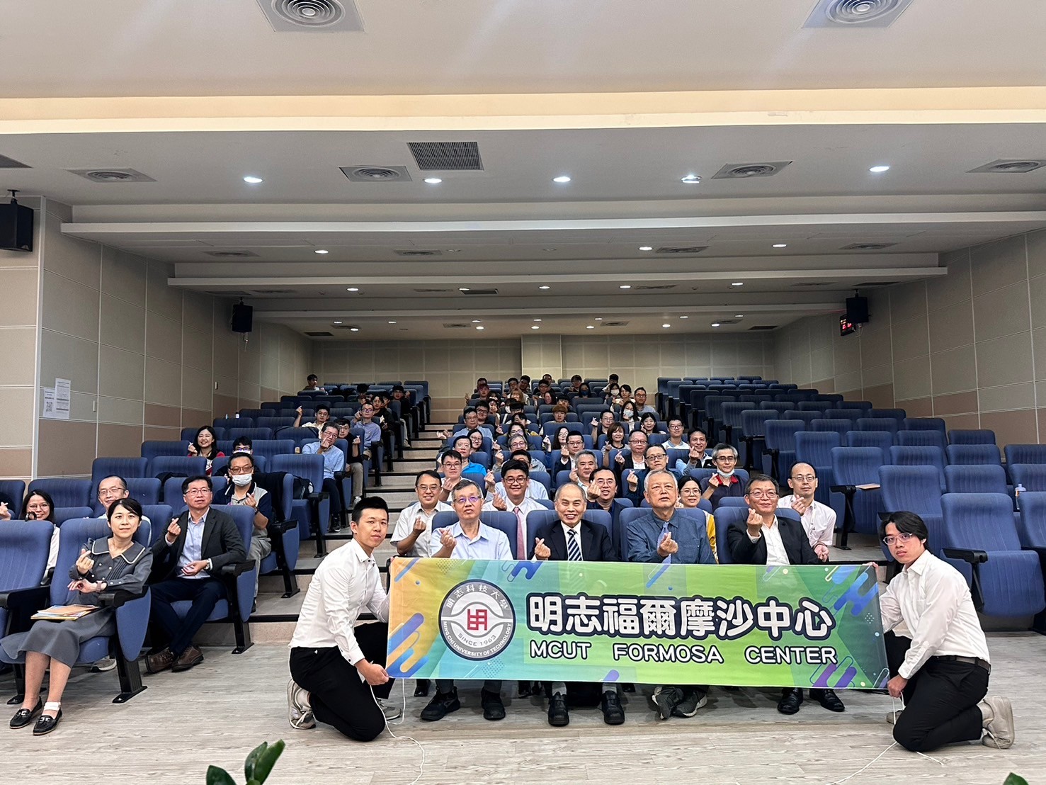
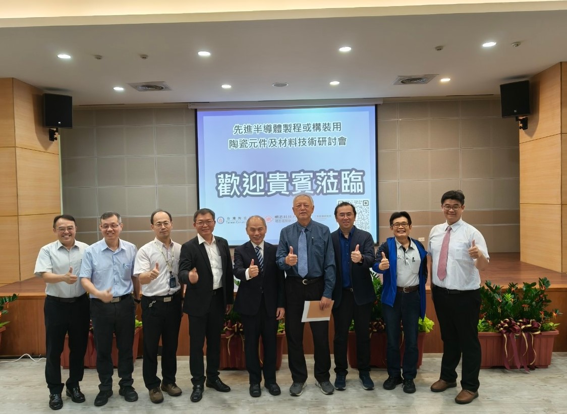
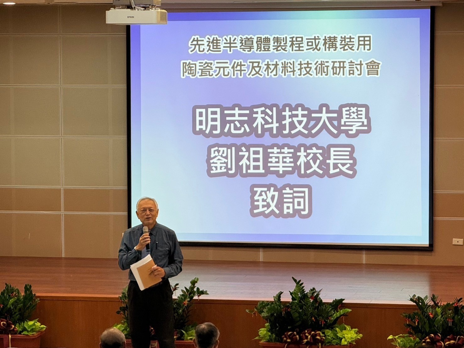
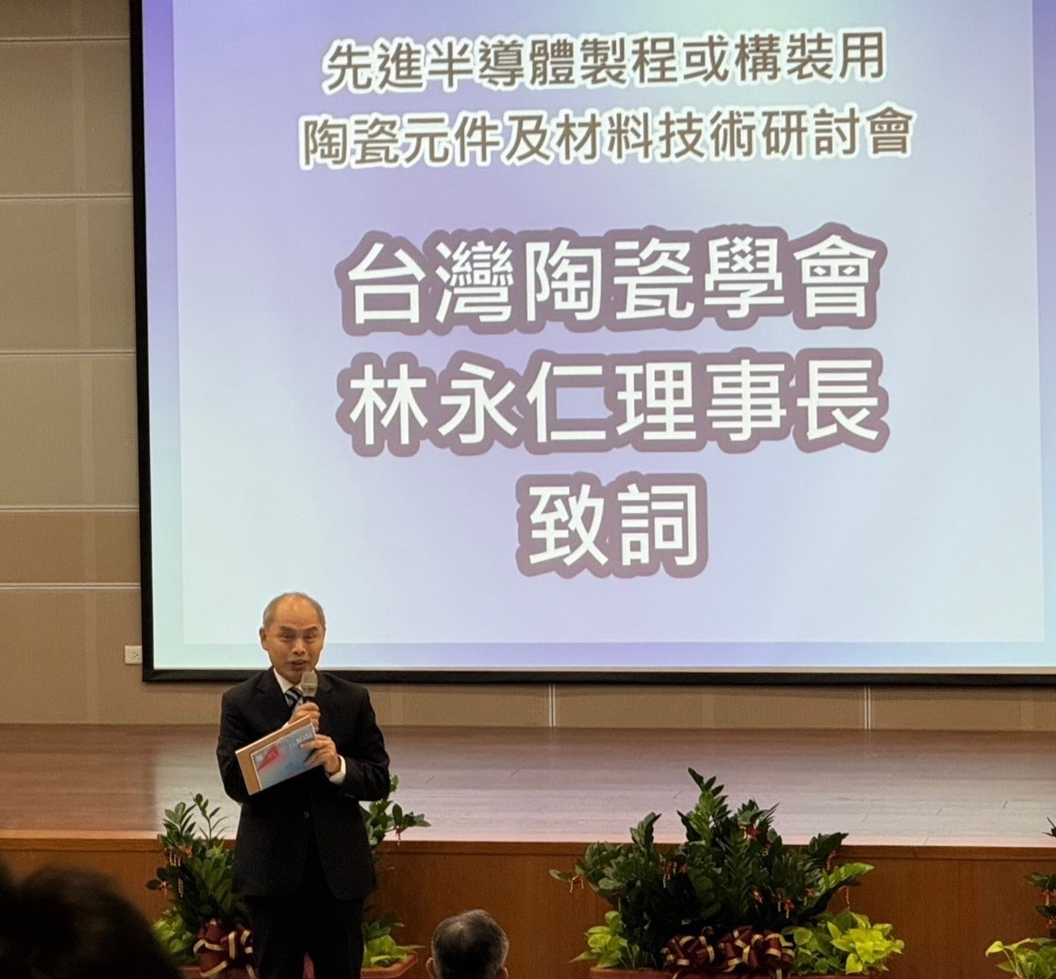
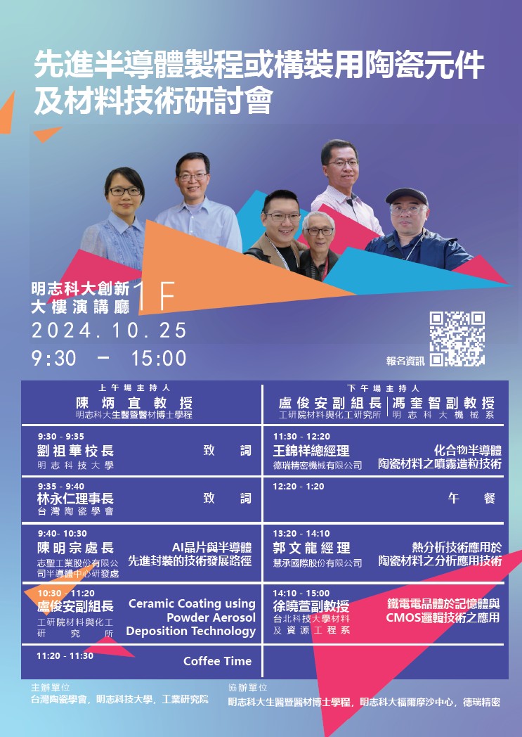
On October 25, 2024, Ming Chi University of Technology, in collaboration with the Taiwan Ceramic Society and the Industrial Technology Research Institute, hosted the "Advanced Ceramic Components and Materials for Semiconductor Processing and Packaging Technology Symposium" on campus. The event attracted over 120 experts and researchers from academia and industry. The symposium aimed to promote the application of ceramic components and materials in advanced semiconductor processing and packaging while providing a platform for innovation and knowledge exchange in the field. Attendees took this opportunity to delve into how ceramic material technology can meet the future needs and challenges of the semiconductor industry.
The symposium featured a rich and varied agenda covering cutting-edge topics in semiconductor technology, beginning with the much-discussed CoWoS (Chip on Wafer on Substrate) packaging technology. Known for its high-performance and high-integration advantages, CoWoS has become a crucial choice in advanced semiconductor processing. This technology enables the integration of multiple functions within a single package, significantly enhancing system performance and computational speed, especially beneficial for high-performance computing applications. Additionally, the symposium provided an in-depth look into ceramic coating deposition technology, which not only enhances the surface protection of semiconductor components but also improves their durability and stability, helping extend component life and reduce costs.
In the field of material processing technology, the symposium also covered powder processing and thermal analysis techniques for semiconductor compound materials. These technologies play a vital role in controlling the physical and chemical properties of materials, ensuring component stability under high-temperature and high-pressure conditions, which is critical for semiconductor manufacturing and applications. Through precise powder processing, the structure and performance of materials can be optimized, while thermal analysis further reveals thermal stability and conductivity properties, laying the foundation for future high-performance semiconductor products.
The symposium showcased advanced technological achievements and facilitated technical exchanges between academia and industry. Participants actively shared insights and experiences in technology development, discussing the potential of ceramic material technology in semiconductor processing and packaging applications. This event strengthened the foundation for collaboration between the industry and academia, providing ample opportunities for future innovations. The success of the symposium highlights the significance of ceramic components and materials technology within the semiconductor industry, guiding future technology development and laying the groundwork for advancements in semiconductor processing.
中文:「技術前沿·陶瓷賦能」——先進半導體製程與構裝陶瓷技術研討會成功舉行
This article is simultaneously published in the 17th edition of the SDGs E-paper.